Modelling of Wide Bandgap Semiconductor Losses
Wide bandgap (WBG) semiconductors, including SiC MOSFETs and GaN HEMTs, enable to operate power devices at much higher voltages, frequencies and temperatures than conventional Si semiconductors. The superior intrinsic properties of WBG semiconductors allow for a wide application in power converters with high power density and high efficiency. For optimally designing such converters, an accurate semiconductor loss model, including conduction and switching losses, is required. Considering the huge computational effort to evaluate different designs over wide operating ranges for converter optimisation, the loss model should be both computationally efficient as well as accurate. As a result, analytical models are usually preferred over physics-based and behavioural models due to their good compromise between accuracy and computational effort.
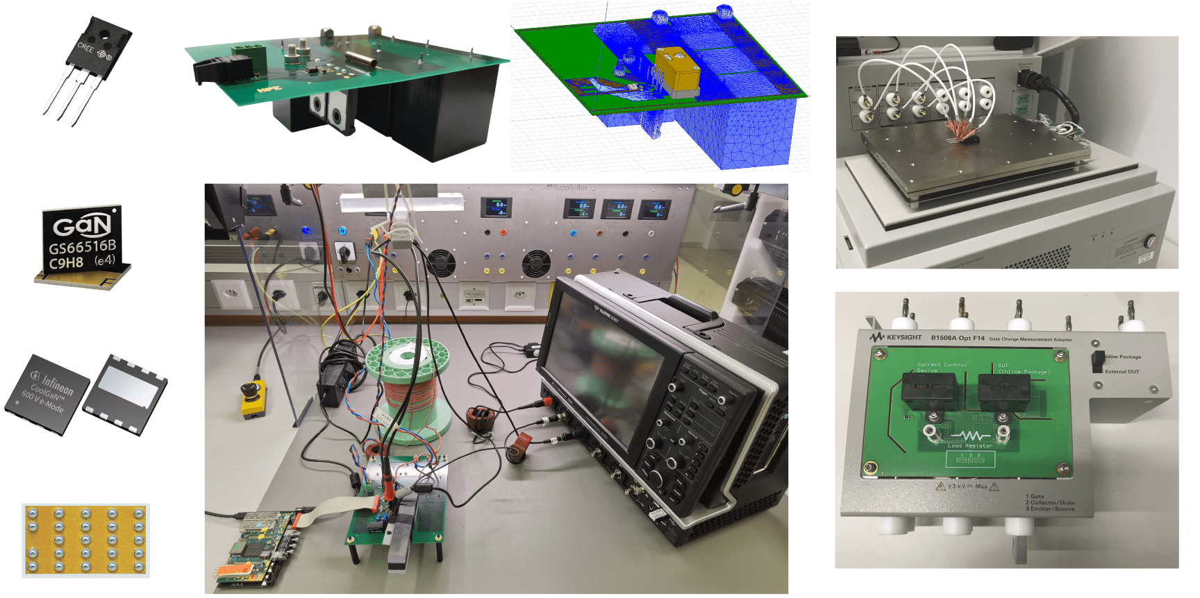
This project aims to develop accurate and computationally efficient loss models for WBG semiconductors, which are valid in a wide range of operating parameters as e.g. voltage, current, and temperature. This requires a deep understanding of both the fundamental semiconductor theories and the impact of the parameters on the switching behaviour with hard or soft switchings. In addition, the relevant parasitics caused by the PCB layout and packaging need to be modelled and are verified by FEM simulations and impedance measurements. Furthermore, accurate loss measurement techniques need to be investigated in order to verify the calculated loss values.