Nanosecond Solid-State Pulse Generator
Pulsed-power techniques have been successfully applied in various areas such as medical treatment, food processing, military equipment, plasma generation and particle accelerator systems. Today, more and more pulse modulators are based on power semiconductor devices instead of hard tube devices, which have been commonly used as high-power electrical switch. The reason for this is the increasing power handling capability and robustness of modern semiconductors. In addition, these semiconductor devices enable the pulse to be turned off in case of faults and are not subject to single source issues.
In the past, high power solid-state pulse modulator systems were mainly designed with the focus on pulse lengths in the range of microseconds to milliseconds due to the limited switching speed of bipolar devices as for example insulated gate bipolar transistors (IGBT) and the limited power handling capability of unipolar devices such as metal-oxide-semiconductor field-effect transistors (MOSFET). Over the past years, the current and voltage handling capability of unipolar devices significantly increased due to the rise of modern wide bandgap semiconductors as for example silicon carbide (SiC) or gallium nitride (GaN). This trend will continue in the future. In addition, unipolar devices can inherently switch much faster than bipolar switches. Therefore, short pulse lengths in the range of a few nanoseconds come into reach of advanced solid-state modulators based on novel semiconductor devices. Such nanosecond pulses are advantageous for example in injection/extraction systems of particle accelerators, medical lasers or systems for plasma ignition.
In the framework of the project, the basic limitations of very fast solid-state pulse modulators in terms of minimal pulse length and of minimal achievable rise/fall times will be comprehensively evaluated. Semiconductors with a relatively low breakdown voltage (around 1 kV or even below) are the main focus of the carried out investigations since the switching times of modern power semiconductors usually decrease with decreasing breakdown voltage. Consequently, the solid-state modulator system will be based on a series connection of several switches or switching modules. In addition, multiple semiconductor dies have to be connected in parallel in order to be able to switch and conduct currents in the range of a few hundred amperes.
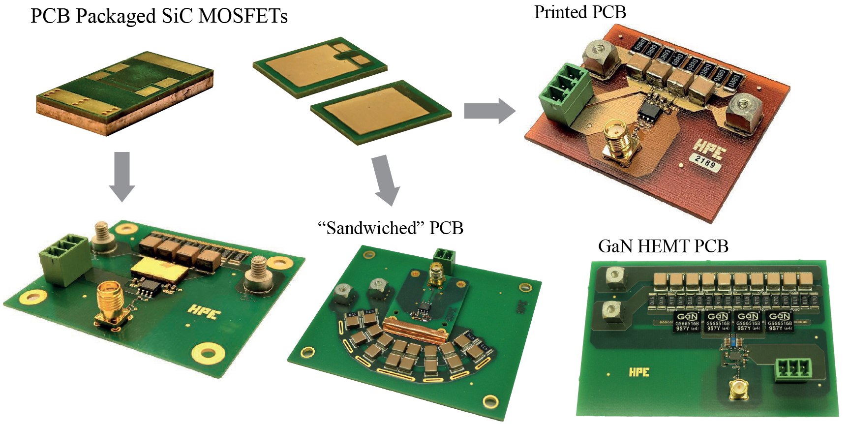
Unipolar devices, including SiC MOSFETs, have a very high intrinsic switching speed. Therefore, the practically achievable switching times are mainly determined by the parasitics of the semiconductor die and its package, the commutation loop and the gate drive loop. Thus, it is very important to identify an integration concept for the switching module that combines the semiconductor switch, the gate drive circuit and the power loop with minimal parasitics. Therefore, advanced semiconductor packaging concepts are also investigated during the project.
On a system level, the solid-state topology with the best pulse performance needs to be selected. Furthermore, the modularity and reliability as well as the scaling to higher power ratings are investigated. The mechanical/electrical layout of the system, i.e. the interconnections between the switching modules, needs to be designed in such a way that an impedance matching between the pulse generator and the load is achieved in order to minimise pulse reflections.